


This website uses cookies so that we can provide you with the best user experience possible. Cookie information is stored in your browser and performs functions such as recognising you when you return to our website and helping our team to understand which sections of the website you find most interesting and useful.

Understanding novel transistor technologies for a more connected world
Support for start-up to characterise Gallium Nitride transistors
Access to the Royce High-Voltage Electrical Characterisation Suite enabled Cambridge GaN devices to characterise transistor prototypes to exploit the new emerging material’s semiconductor capabilities.
Cambridge GaN Devices (CGD) develop novel Gallium Nitride (GaN) power devices with transistors that can switch high voltages and currents over 100 times faster than the best-selling commercial silicon MOSFET (metal–oxide–semiconductor field-effect transistors) while guarantying reliable operation compared to the existing GaN solutions.
GaN transistors have the capability to replace silicon in everything from consumer electronics, chargers, data servers to solar inverters. The devices take advantage of the tremendous properties of GaN such as the higher critical electrical field, the extremely high electron-mobility, and low on-state resistance. This delivers efficient power transistors which are less hot and therefore require significantly smaller cooling and enable higher power densities than silicon equivalents.
The Challenge
CGD is a fabless GaN semiconductor industry and the transistors fabricated by their foundry partners need careful and extensive characterisation. This includes the test of the static and dynamic performance of the transistors. In particular, temperature-dependent tests and high-voltage tests are crucial to the understanding of the underlying physical effects in the devices related to crystal defects and traps typical of GaN-based transistors.
Support from the Henry Royce Institute
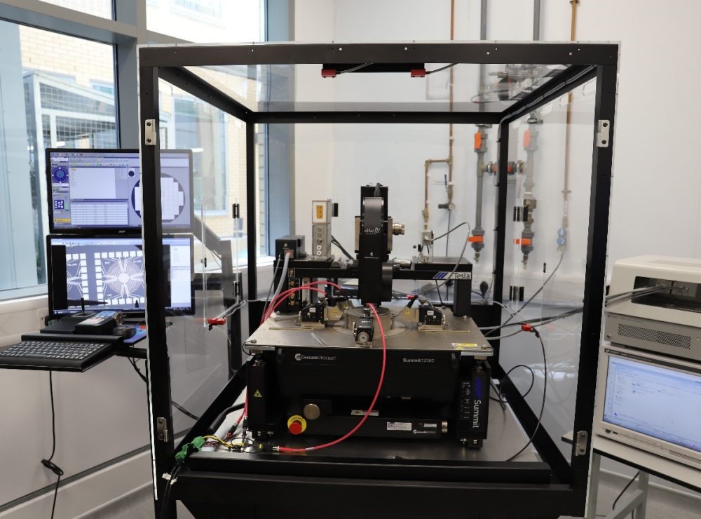
As part of the Accelerator Token scheme, CGD received funding to access the High-Voltage Electrical Characterisation Suite of the Henry Royce Institute based at the University of Cambridge.
The probe station enables CGD to automatically contact every single transistor on a wafer. Once contacted, the Semiconductor Parameter Analyser will test the device in detail. Further, the equipment puts CGD in a position to measure packaged devices after encapsulation; be it for prototypes or production samples.
The results will allow CGD to further optimise their proposition, demonstrate the unique advantage of their technology and get one step closer to the market.
* By March 2020 the Royce Accelerator Token Scheme will have supported 21 projects from Start-up and SME businesses with access to equipment and expertise to run proof-of-concept and feasibility studies.