


This website uses cookies so that we can provide you with the best user experience possible. Cookie information is stored in your browser and performs functions such as recognising you when you return to our website and helping our team to understand which sections of the website you find most interesting and useful.
Supporting the Development of Low-loss Electronics through Harsh Chemical Environmental Testing for Semi-Conductor Materials
Case Study
Overview
Every material introduced in semiconductor manufacturing can become an airborne molecular contaminant (AMC). However, the most common sources are off-gassing of cleanroom building materials and fugitive emissions from wafer processing. With the surge in demand for semiconductor materials and devices, they are often produced at the nanoscale making them considerably more susceptible to degradation from impurities.
Therefore, in-process metrology underpinned quality control is required to ensure high-grade, high throughput production. In this project, the research team demonstrated capabilities that highlight the impact of gaseous AMCs on semiconductor materials through controlled contamination and subsequent defect characterisation. The development of the technology is integral for enabling efficient UK manufacturing and supporting the rapid development of new technologies such as low-loss electronics.
About The Project
The highest costing defect is the one not detected in real-time. For a wafer manufacturing facility with a monthly run rate of 25 000, defect detection at the end of process rather than in-operando resulting in one in four wafers being scrapped would accumulate to a staggering £21 million yield loss per incident. This is further emphasised by the NACE International report estimating advanced manufacturing’s global revenue loss due to defective parts at $17.6 billion.
There are many studies examining semiconductor components at elevated temperature and pressure or looking at particle contamination. However, no metrology projects have been conducted in chemically hostile gaseous environments.
To address this, in this project the research team developed the first method for in-situ harsh chemical environmental testing to assess the impact of trace level AMCs on semiconductor materials. In this pilot study, Gallium Arsenide (GaAs) and Indium Phosphide (InP) wafers were exposed in controlled contamination to one of the most prominent cleanroom AMC – hydrogen chloride (HCl). Three amount fractions were selected in the range of 1 – 10 nmol mol-1 utilising NPL’s expertise on generating and measuring trace levels of HCl.
The two wafer materials were introduced independently into the reaction chamber and contaminated with the three different HCl concentrations. The HCl absorption was monitored online using a cavity ringdown spectroscopy (CRDS) analyser, measuring approximately 10 % concentration decrease correlated to reaction of the contaminant with the materials.
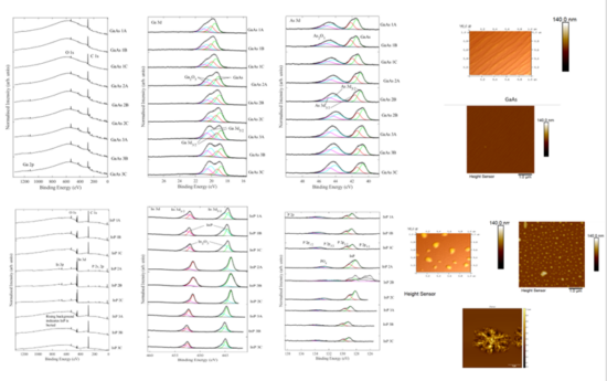
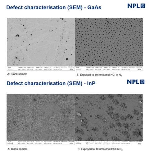
Defect characterisation was performed by the Royce team at the University of Manchester. The group provided technical expertise and valuable insight into the topography and morphology of the samples by utilising a combination of spectroscopy and microscopy techniques. Blank samples were analysed using AFM allowing for differentiation between contamination defects and substates distribution. They were further processed with HAXPES and TEM, which confirmed the formation of surface oxidation layer with 10 nm thickness on both wafer materials due to testing in laboratory conditions rather than in cleanroom ones.
Studies demonstrate that this protective oxide barrier could be removed readily by exposing the wafers to mild acid. As such, HCl reacted with the oxide.
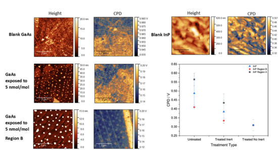
However, at approximately 1 nmol mol-1 level, it was insufficient to further react with the substrate. Crystalline structures formation on the surface was observed using SEM, after contamination with 5 and 10 nmol mol-1. In InP they appeared as structure growths whereas for GaAs etch pits were observed. The defect formations were further emphasised by the decrease in electric potential and increase in surface roughness, measured by KPFM.
The promising preliminary results demonstrated throughout pilot study allow for utilisation of the new facility developed as an innovation acceleration platform for new and existing materials across numerous UK businesses. Its further advancement would benefit the industry by providing understanding of the cause-effect relationship between manufacturing parameters and defects.
It will also result in environmental and societal benefits by providing optimised cost-to-benefit ration via a reduced scrap rate and an increased yield, minimised energy waste consumed during manufacturing and improved quality of life through the production of defect-free semiconductor components.
“With the increasing miniaturisation of semiconductor devices, it is becoming more important to understand how impurities cause defects and faults. This project developed new capabilities that can support the semiconductor manufacturing industry to have greater confidence in the quality of their products. This in turn will provide reliable, higher quality, lower cost products in sectors utilising semiconductor materials, support the development of new technologies directly benefiting UK’s citizens and contribute to an optimized cost-to-benefit ratio by reducing scrap material rates resulting in minimal environmental impact from production.”
Yoana Hristova MChem MRSC
Higher Scientist
NPL Management Limited
Collaborators
The work was completed with lead organisation NPL Management Limited, working with partners at Compound Semiconductor Centre Limited.
The work was enabled due to a grant from the Henry Royce Institute’s Industrial Collaboration Programme, utilising facilities at the Royce Hub at the University of Manchester.