

This website uses cookies so that we can provide you with the best user experience possible. Cookie information is stored in your browser and performs functions such as recognising you when you return to our website and helping our team to understand which sections of the website you find most interesting and useful.
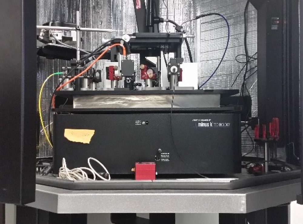
Bespoke variable-temperature diamond sensing system operating from 4 K to 300 K, 9T out-of-plane superconducting magnet, with spatial resolution of ~50 nm
Variable Temperature Nanoscale Sensing and Imaging system
This system uses atomic defects in bespoke all-diamond scanning probes to probe the local magnetic field from a static magnetisation or current with a spatial resolution of ~50 nm.
- Partner:University of Cambridge
- Facility:Cavendish Laboratory
- Availability:Available
Or call us now on 0161 275 8382
Detailed Description
The dynamic range of the system spans DC to MHz with sub mT sensitivity for the magnetic sensing modes respectively. The imaging system is housed in a temperature-controlled and vibrationally isolated housing, which enables <0.5 K temperature stability and <5 nm drifts over the course of several hours.
Uses/Applications
Owing to the single-spin nature of the nitrogen-vacancy defect, this system is ideal for imaging emergent magnetic and transport phenomena in low dimensional materials such as skyrmions, magnons, and edge currents, with virtually no perturbation. It can also be used for the fingerprinting of integrated circuit activity, enabling measurements and characterisation of devices for energy-efficiency during testing operations as well as device tampering detection.
The system operates from 4 K to 300 K, with a 9T out-of-plane superconducting magnet, with spatial resolution of ~50 nm.