
This website uses cookies so that we can provide you with the best user experience possible. Cookie information is stored in your browser and performs functions such as recognising you when you return to our website and helping our team to understand which sections of the website you find most interesting and useful.
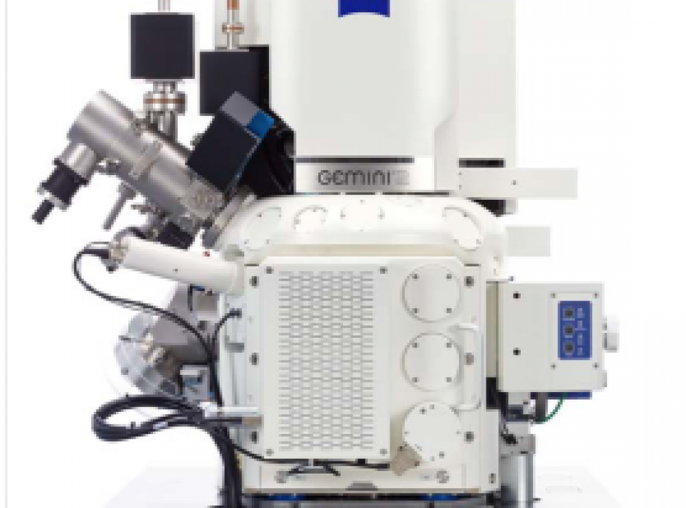
AJA sputter deposition system / Zeiss Cross-beam 540 focused ion beam/electron beam system
Sputter Deposition / Nanoscale Patterning Suite
Users can combine physical vapour deposition and nano-patterning and growth of metallic structures for devices. As a combined suite, these two systems offer the capability for 3D heterostructure device fabrication for magnetic and optical materials systems.
- Partner:University of Cambridge
- Facility:Department of Materials Science
Or call us now on 0161 275 8382
Detailed Description
The sputtering system has numerous targets for the growth of complex metallic heterostructures for devices. The dual beam FIB-SEM system offers an alternative to the standard subtractive etch process used in optical lithography. This system can produce smaller devices without breaking vacuum, and without forming ex-situ interfaces.
Uses/Applications
Heterostructure device fabrication for a range of magnetic and optical materials systems
The AJA sputterer contains a load-lock and is configured with eleven targets, internal calibration, and automated processes. The dual-beam SEM-FIB system uses a range of ion sources including a Ga ion beam to enable direct patterning of micro- and nano-pillar devices.