
This website uses cookies so that we can provide you with the best user experience possible. Cookie information is stored in your browser and performs functions such as recognising you when you return to our website and helping our team to understand which sections of the website you find most interesting and useful.
Imaging at high resolution; milling features into sample surface
- Partner:UK Atomic Energy Authority
- Facility:Materials Research Facility (MRF)
- Availability:Available
Or call us now on 0161 275 8382
Detailed Description
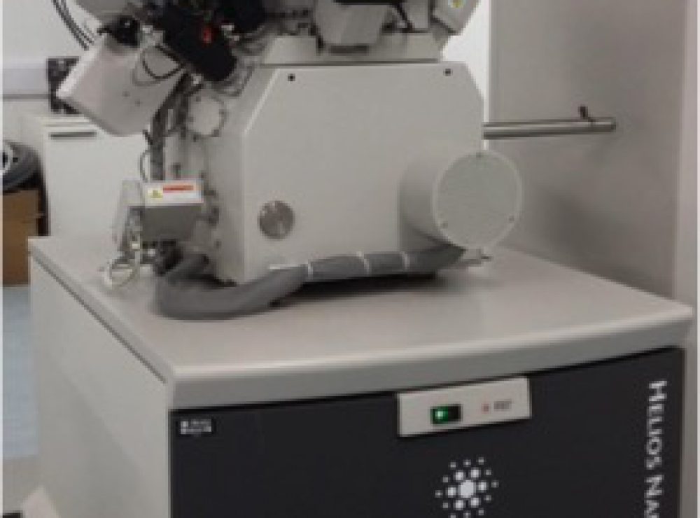
The Focused Ion Beam (FIB) is a dual beam system, meaning it can image at high resolution using an electron beam, as well as mill features into the surface of a sample using a high-energy gallium ion beam to remove material via sputtering. In addition, a precise manipulator needle enables micron-scale specimens to be lifted out of the sample surface.
Uses/Applications
Micro-machining using the FIB enables site-specific examination of a sample. Mechanical test pieces, such as pillars for compression or cantilevers for bend tests, can be manufactured as well as thin films, which can then be taken away for microstructural characterisation in a transmission electron microscope.
FEI Helios NanoLab 600i
Schottky thermal field-emission electron gun, 1.4 nm resolution at 1 kV
Gallium ion source for milling, 4.5 nm resolution at 30 kV
Voltage ranges and probe currents
Electron-beam: 350 V – 30 kV, 0.7 pA – 22 nA
Ion-beam: 500 V – 30 kV, 0.1 pA – 65 nA
Magnification
1x – 1,000,000x
High-precision, 5-axes motorized stage
Gas injection system
Platinum deposition
Tungsten deposition
Carbon deposition
Easy lift nano-manipulator
Drift < 50 nm/minute
Minimum step size 50 nm
True ‘z’ movement
Vibration < 15 nm