
This website uses cookies so that we can provide you with the best user experience possible. Cookie information is stored in your browser and performs functions such as recognising you when you return to our website and helping our team to understand which sections of the website you find most interesting and useful.
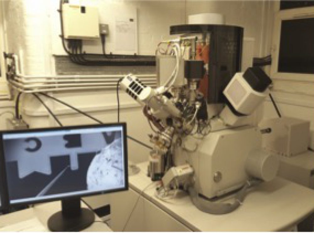
Extreme high-resolution (XHR) Field Emission Scanning Electron Microscope (FE SEM)
- Partner:The University of Manchester
- Facility:Multidisciplinary Characterisation Facility (MCF)
Or call us now on 0161 275 8382
Detailed Description
The FEI HELIOS 660i Nanolab FIB with Oxford EBSD & EDSsystem is a high-resolution Focused Ion Beam (FIB) system equipped with extreme high-resolution (XHR) Field Emission Scanning Electron Microscope (FE SEM). It also has a large area high-efficiency EDS detector for local elemental chemistry. High-speed, high-precision EBSD detector for sample crystallographic analysis in one system.
Uses/Applications
This is a unique and versatile characterisation tool. It allows for the precise characterisation of nanometer details and analysis in 2D and 3D, very high quality sample preparation and flexible nanoprototyping.
Ion beam
Field emission focused ion beam optics with liquid Gallium ion emitter.
Voltage: 0.5 kV to 30 kV
Beam current: 0.1pA – 65nA
Resolution: 4.0 nm at 30 kV
Electron optics
Dual-mode magnetic immersion / field free lens electron optics with ultra-high brightness
Source: Schottky field emitter
Landing energies: 20 V to 30 kV
Beam current: 0.8 pA – 100 nA
Resolution: 0.6 nm at 15 kV
Scanning
Up to 6144×4096 pixels
Patterning
Resolution: 64k x 64k
Pattern size: 8M pixels
Variable dwell time pattern to give 3D milling
Complex milling patterns through Bitmap import