This website uses cookies so that we can provide you with the best user experience possible. Cookie information is stored in your browser and performs functions such as recognising you when you return to our website and helping our team to understand which sections of the website you find most interesting and useful.
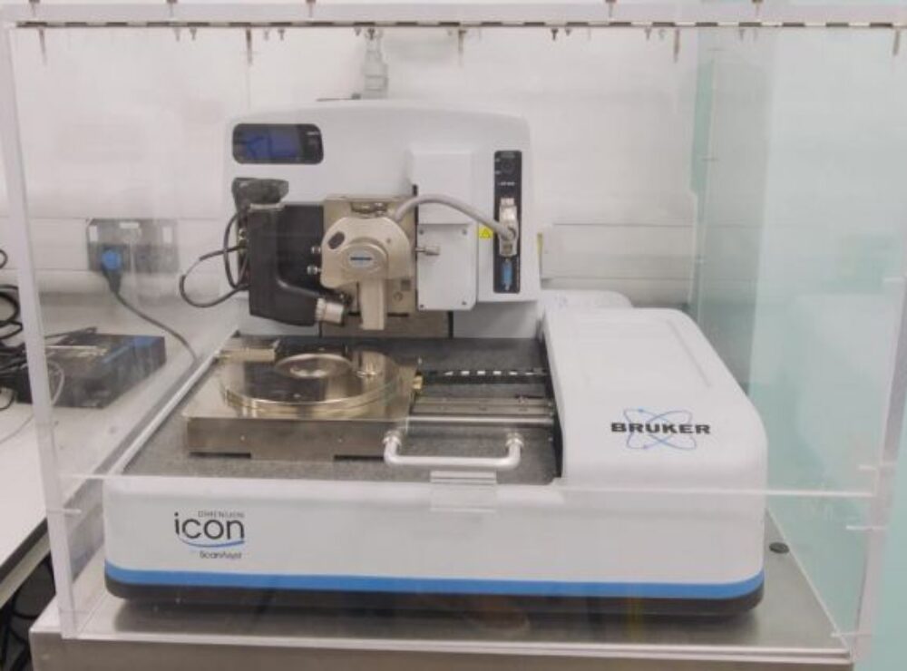
The Bruker Dimension Icon is a cutting-edge AFM with a full electrical package for comprehensive nanoscale characterization. It delivers high-resolution imaging and advanced electrical measurements, making it ideal for materials science, semiconductor research, and nanotechnology.
- Partner:The University of Sheffield
- Facility:Royce Discovery Centre
- Availability:Available
Or call us now on 0161 275 8382
Detailed Description
The Bruker Dimension Icon is renowned for its exceptional performance, flexibility, and precision. Its design ensures robust performance even in demanding environments, making it suitable for both routine and advanced research tasks. With a large scan range of up to 90 µm x 90 µm and a vertical range of up to 10 µm, the Dimension Icon can handle a wide variety of sample sizes and types, providing flexibility that is often unmatched by other AFMs. Our instrument is enhanced with advanced electrical modes extensions, significantly increasing its versatility beyond standard configurations.
Uses/Applications
Molecular structures and interactions, surface topography and mechanical properties, conductivity and magnetic properties, ferroelectric and piezoelectric materials, corrosion analysis, nanodevice fabrication, battery research, fuel cells, photovoltaics and supercapacitors, etc.
Max. sample size: 210mm diameter and 15mm thickness.
Max. size of a single scan: 90μm x 90μm with 10μm Z range.
Working environment: Air.
In-situ optics: Top view camera.
Imaging modes: Contact Mode, Tapping Mode, ScanAsyst, PeakForce QNM, Force Spectroscopy and Force Volume, Conductive AFM (cAFM), Electrostatic Force Microscopy (EFM), Magnetic Force Microscopy (MFM), Piezo Response Microscopy (PFM), Tunneling AFM (TUNA) with DataCube (both contact and PeakForce tapping based), Kelvin Probe Force Microscopy (KPFM) (both tapping and PeakForce tapping based).