
This website uses cookies so that we can provide you with the best user experience possible. Cookie information is stored in your browser and performs functions such as recognising you when you return to our website and helping our team to understand which sections of the website you find most interesting and useful.
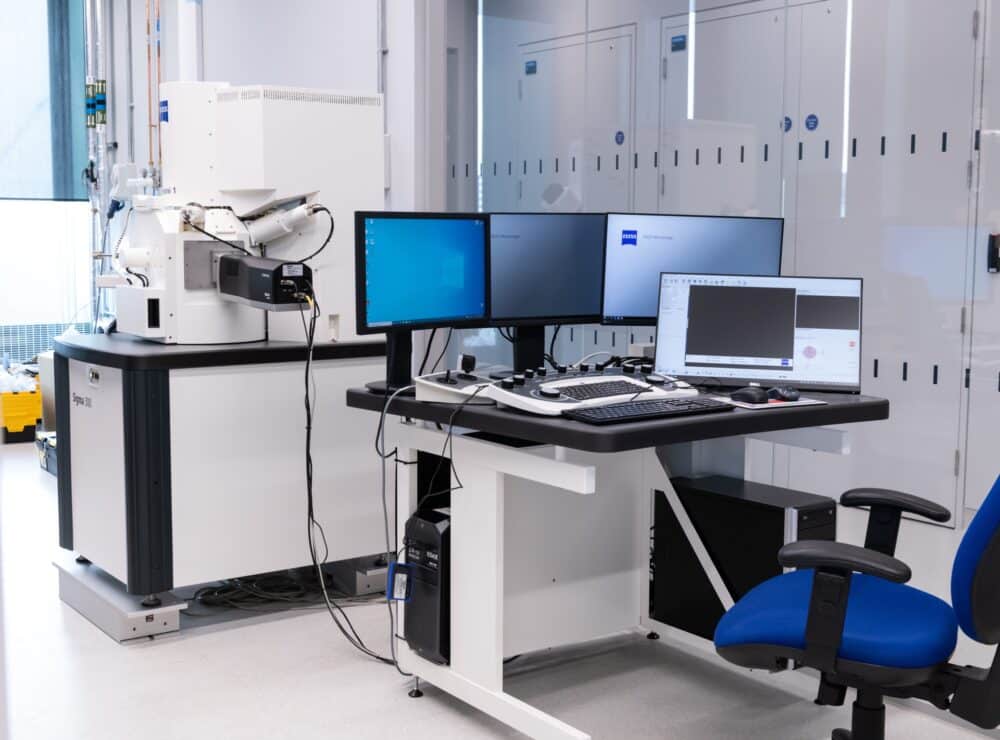
Field emission Scanning Electron Microscope (SEM)
- Partner:Imperial College London
- Facility:Thin Film Technology Laboratory
- Availability:Available
Or call us now on 0161 275 8382
Detailed Description
Combine field emission SEM (FE-SEM) technology with analytics. Profit from proven Gemini electron optics. Choose from a variety of detector options: image particles, surfaces, and nanostructures in materials science investigate semiconductor or medical devices, and geological or biological samples.
Save time with the semi-automated 4-step workflow of Sigma: structure your imaging and analysis routines and increase productivity. FE-SEM users of all disciplines in research and industry labs now benefit from a resolution of 1.3 nm at 1 kV in ZEISS Sigma 500 and better usability.
Uses/Applications
Imaging for thin film process control