This website uses cookies so that we can provide you with the best user experience possible. Cookie information is stored in your browser and performs functions such as recognising you when you return to our website and helping our team to understand which sections of the website you find most interesting and useful.

Research Area
Atoms to Devices
Vision
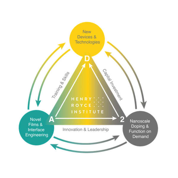
The vision of the ‘Atoms to Devices’ (A2D) Research Area is to provide the underpinning, cross- disciplinary, technology platforms to facilitate and support the accelerated discovery and development of new device materials. Through the deposition of precisely controlled thin films, the engineering of
interfaces, and the ability to control doping on the nanoscale, it enables the design of new devices and new technological solutions that underpin a breadth of societal applications.

Above: watch Professor Neil Alford introduce the Atoms to Devices Research Area.
Introduction and Scope
Atoms to Devices is the quantum scale engineering of new technologies, that can translate into applications ranging from photonics, imaging, semiconductors and sensors, through to energy storage, biomedical materials and quantum technologies.
The research area comprises modelling, design, growth, fabrication, characterisation, and testing of electronic, spintronic and opto-electronic devices.
The common thread that runs through the Atoms to Devices theme is the deposition of thin films, their fabrication into devices, their characterisation both chemically and structurally (XRD, Raman, XPS, EPMA) and their electrical testing, exploring the response of films exposed to electromagnetic fields from DC, through microwave and terahertz, to optical frequencies.
Current and Future Research
- Development of electronic materials for the energy transition to meet net zero carbon targets by 2050, including research into photovoltaics, calorics and thermoelectrics, and low-loss electronics.
- Demonstration of efficient catalysts to support carbon-free hydrogen generation.
- Development of new device paradigms, including ‘chargeless’ electronics, new computing architectures, and quantum technologies.
- Design of bioelectronic sensors to support personalised healthcare, and clinical assessment.
- Development of resource abundant, scalable and recyclable materials.
Links
- South Wales Semiconductor Cluster
- Materials for the Energy Transition
- Centre for Centre for Quantum Computing and Communication Technology (CQC2T)
- UK Quantum Technology Hubs

Equipment & Facilities
Located at the University of Leeds, the new Bragg Centre is a £96m development to create an integrated campus for Engineering and Physical Sciences. Located on the north east quarter of the University campus, the 15,700m² building fosters a culture of inter-disciplinary working in the development of novel materials to address 21st Century challenges in many areas, including energy efficient computing, telecommunications, sustainable magnetic materials, sensors for use in biological systems and extreme or remote environments, pharmaceutical formulations, ‘smart foods’ and medical technologies. The facility includes first-class laboratory and specialised teaching spaces, enabling cutting-edge research, and outstanding student experience, whilst enhancing the University’s research power and strengthening collaboration with industry.
The University of Cambridge’s Maxwell Centre is the centrepiece for industrial engagement with the physical scientists and engineers working on the West Cambridge Science and Technology Campus. The two-way flow of ideas and researchers adds value when ‘blue-skies’ activities meet research objectives relevant to economic opportunities for industry and society at large, with the scale of industrial involvement already being substantial. A2D research at Cambridge centres around the ambient cluster tool for the growth, characterisation, testing and packaging of novel devices, as well as our E-Beam lithography, XPS, MBE facilities and a suite of associated equipment supporting the development of low-loss electronics and high energy-density storage materials.
At Imperial College London, the university is providing state-of-the-art facilities dedicated to the innovation of novel multifunctional devices. Royce Atoms to Devices researchers have access to facilities for nano-scale thin film deposition, device patterning and electrical characterisation and instrumentation able to analyse of a wide range of surfaces, along with a range of tools for prototyping nano-devices.

